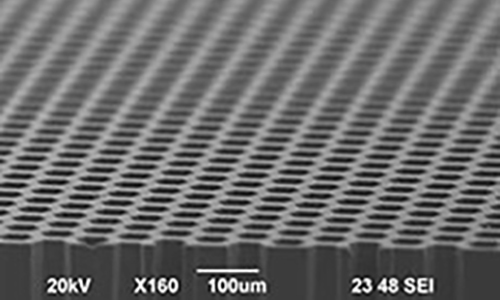
Photolithography is a critical procedure in semiconductor device manufacturing. It patterns device structures on photoresist layers via exposure and development, then transfers patterns from masks onto substrates through etching. Meiming Electronics masters multiple photolithography technologies including electron beam lithography, stepper lithography and contact lithography.
Process Introduction
Photolithography is a critical procedure in semiconductor device manufacturing. It patterns device structures on photoresist layers via exposure and development, then transfers patterns from masks onto substrates through etching. Meiming Electronics masters multiple photolithography technologies including electron beam lithography, stepper lithography and contact lithography.
Technical Applications
Photolithography technology is mainly applied in the fabrication of semiconductor devices and integrated circuits.
Applicable Materials
Silicon wafer, glass, sapphire, flexible materials, etc.
Process Capacity
Electron Beam Lithography (EBL): Minimum line width 50nm, precision up to 10%.
Stepper Lithography: Stepper i7/i10/i12, minimum line width 350nm, exposure error ±0.1um.
Contact & Proximity Lithography: MA6/BA6 mask aligner, minimum line width 1um, exposure error ±0.5um.
UV lithography, maskless lithography, double-side lithography, alignment & overlay exposure; supported wafer sizes: 8", 6", 4", 2" and irregular small chips